Elon Musk launched TeraFab in late March 2026 with $20 billion in initial funding. The stated goal is to manufacture logic chips, memory, and advanced packaging all under one roof, an integrated chipmaking operation that no company on earth currently runs at scale. The $20 billion is a starting point. What Musk actually wants to build would cost 250 times that.
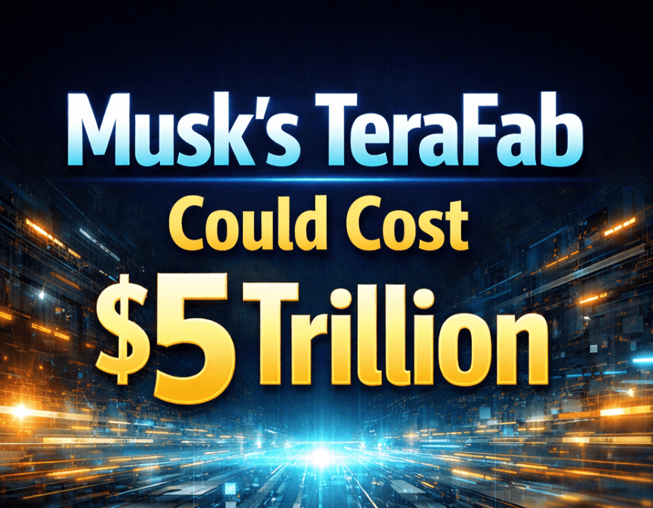
Investment research firm Bernstein ran the numbers. To hit Musk's stated ambition of producing AI chips that consume one terawatt of power annually, TeraFab would need between 142 and 358 modern semiconductor fabs. The total price tag: approximately $5 trillion. For context, the entire US federal budget this year is around $7 trillion.
What the math actually looks like
The terawatt target is not a vague aspiration. Musk has said publicly he wants foundry partners, and now his own facilities, to produce hundreds of billions of AI chips per year. Bernstein translated that into wafer demand: roughly 22.4 million Rubin Ultra GPU wafers, 2.7 million Vera CPU wafers, and 15.8 million HBM4E memory wafers annually.
A modern leading-edge logic fab produces around 20,000 wafer starts per month, or about 240,000 wafers per year. At 80% yield, hitting the GPU and CPU wafer targets alone would require approximately 126 logic fabs. Each 2nm-class fab costs between $25 billion and $35 billion to build. Logic capacity alone comes to somewhere around $3.15 to $3.78 trillion, before a single memory chip is made.
Memory is a separate problem. HBM production requires DRAM fabs running at 100,000 to 200,000 wafer starts per month. Producing 15.8 million HBM wafers annually would need around 9 to 12 dedicated DRAM facilities at $20 billion each, adding roughly $240 billion to the bill. Then there is advanced packaging, the facilities that stack HBM onto processors using 2.5D and 3D integration. These run $2 to $3.5 billion per phase, and TeraFab would need tens to hundreds of them.
Add land, R&D, software infrastructure, and workforce, and the total exceeds $4 trillion by a wide margin. Bernstein's $5 trillion figure, while rough, is directionally conservative.
To put $5 trillion in perspective
Nvidia's market cap as of early 2026 sits at around $4.34 trillion. Apple is at $3.71 trillion. Alphabet is at $3.5 trillion. Musk would need to mobilize capital exceeding the value of the world's most valuable company to build what he is describing. Even if the US government wanted to fund it entirely, doing so would consume more than 70% of its annual budget in a single appropriation.
TSMC, the world's most advanced chipmaker, shipped 15 million 300mm-equivalent wafers across all its process nodes in all of 2025. It took the company over two decades and roughly 50 fab modules to reach that capacity. TeraFab is proposing to build more than twice that output, from scratch, on an unspecified timeline.
The constraints that money cannot solve
Even setting aside the financing problem, which is itself probably insurmountable for a private venture, there are hard physical limits that $5 trillion cannot simply override.
ASML, the Dutch company that makes the extreme ultraviolet lithography machines required for cutting-edge chip production, ships roughly 50 to 60 EUV machines per year globally. Every major chipmaker is already competing for that allocation. A buildout of 100-plus leading-edge fabs would require hundreds of EUV machines over a compressed timeline. That supply does not exist.
Skilled semiconductor engineers and fab technicians are already in short supply globally. Samsung, Intel, and TSMC are all struggling to staff their existing expansions in the US, Germany, and Japan. A TeraFab buildout at the scale Musk describes would require a workforce that simply has not been trained yet.
Construction materials, ultrapure water systems, power infrastructure, and chemical supply chains for photoresists and process gases are all similarly constrained. Building one leading-edge fab takes four to five years under normal circumstances. Building 126 of them simultaneously is not a scheduling problem. It is a civilizational-scale industrial mobilization.
What TeraFab actually is right now
The $20 billion announced at launch is barely enough to build a single 7nm-class logic fab, a process node that TSMC commercialized in 2018. Tesla is currently hiring a semiconductor fabs construction manager, which suggests the project is in very early planning stages.
The gap between where TeraFab starts and where Musk says it is going is not a gap that gets bridged through ambition or capital efficiency. It is a gap that would require a coordinated, multi-decade effort across governments, sovereign wealth funds, equipment makers, and capital markets simultaneously, all betting on a single private venture run by someone with seven other major companies competing for his attention.
Musk's ambitions for TeraFab are also somewhat self-serving. Tesla, SpaceX, and xAI are all voracious consumers of compute. Vertical integration into chipmaking would reduce dependency on TSMC and Nvidia, both of which represent real strategic risks for his businesses. That framing makes TeraFab rational as a hedge. As a plan to reshape the global semiconductor industry, the numbers do not come close to adding up.
The $20 billion is real. The $5 trillion is the actual cost of what Musk says he wants. The distance between those two figures is the most important fact in this story.
---
Join Newnex - the exclusive platform for institutional VCs to syndicate, co-invest and follow-on privately without intermediaries. www.newnex.io